
sales@north-bridges.com
86-13862120662
Key Specifications
1. RF capabilities
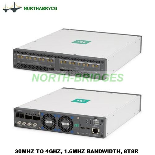
1.1 Up to 8TX, 8RX, independently tunable
1.2 Direct sampling transceiver
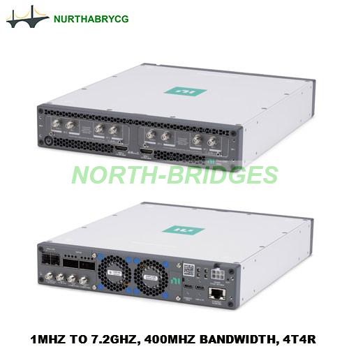
1.3 30 MHz to 4 GHz
1.4 Up to 1.6 GHz bandwidth per channel
1.5 Up to 3.2 GHz aggregated bandwidth per USRP
2. Processing system (PS)
2.1 Quad Core ARM Cortex-A53 (1200 MHz)
2.2 4GB DDR4
3. Programmable logic (PL)
3.1 FPGA: RFSoC ZU28DR
3.2 2X4GB DDR4
Universal X440/X410 Specifications
Key Specifications
| RF capabilities | 8 TX, 8 RX, independently tunable | ||||||||
| Direct sampling transceiver | |||||||||
| 30 MHz to 4 GHz | |||||||||
| Up to 1.6 GHz bandwidth per channel | |||||||||
| Up to 3.2 GHz aggregated bandwidth per USRP | |||||||||
| Processing system (PS) | Quad Core ARM Cortex-A53 (1200 MHz) | ||||||||
| 4GB DDR4 | |||||||||
| Programmable logic (PL) | FPGA: RFSoC ZU28DR | ||||||||
| 2 × 4 GB DDR4 | |||||||||
| Software | UHD version 4.5 or later | ||||||||
| RFNoC | |||||||||
| GNU Radio | |||||||||
| C/C++ | |||||||||
| Python | |||||||||
| OpenEmbedded Linux on A53 | |||||||||
| Synchronization | REF IN (clock reference input) | ||||||||
| PPS IN (PPS time reference) | |||||||||
| TRIG IN/OUT | |||||||||
| GPSDO included | |||||||||
| OCXO included | |||||||||
| Sync In Port (for future use) | |||||||||
| Digital interfaces | 2 QSFP28 (10/100 GbE) | ||||||||
| Ethernet (1 GbE to PS) | |||||||||
| 2 USB-C (USB to PS, Console/JTAG) | |||||||||
| 2 HDMI (GPIO) | |||||||||
| Power, form factor | 12 V DC, 16 A maximum | ||||||||
| Half-wide RU | |||||||||
| 28.5 cm × 22.2 cm × 4.4 cm | |||||||||

USRP X440 Connector Pinout
| Table 1. Front Panel Connector Descriptions | |||||||||
| Connector | Description | ||||||||
DB0, DB1 | RF0 | RX 1 | Input terminal for the RF signal. RX 1 is an MMPX (f) connector with an impedance of 50 Ω and is a single-ended input channel. | ||||||
| TX/RX 0 | Output and input terminal for the RF signal. TX/RX 0 is an MMPX (f) connector with an impedance of 50 Ω and is a single-ended input or output channel. | ||||||||
| RF1 | RX 1 | Input terminal for the RF signal. RX 1 is an MMPX (f) connector with an impedance of 50 Ω and is a single-ended input channel. | |||||||
| TX/RX 0 | Output and input terminal for the RF signal. TX/RX 0 is an MMPX (f) connector with an impedance of 50 Ω and is a single-ended input or output channel. | ||||||||
| SYNC IN | Input terminal for an external IF signal, which is distributed to all four ADCs. SYNC IN is an MMPX (f) connector. SYNC IN accepts signal frequencies up to 1.3 GHz and maximum input power of +15 dBm. | ||||||||
| RF2 | RX 1 | Input terminal for the RF signal. RX 1 is an MMPX (f) connector with an impedance of 50 Ω and is a single-ended input channel. | |||||||
| TX/RX 0 | Output and input terminal for the RF signal. TX/RX 0 is an MMPX (f) connector with an impedance of 50 Ω and is a single-ended input or output channel. | ||||||||
| RF3 | RX 1 | Input terminal for the RF signal. RX 1 is an MMPX (f) connector with an impedance of 50 Ω and is a single-ended input channel. | |||||||
| TX/RX 0 | Output and input terminal for the RF signal. TX/RX 0 is an MMPX (f) connector with an impedance of 50 Ω and is a single-ended input or output channel. | ||||||||
| GPIO 0, GPIO 1 | General Purpose Input / Output (GPIO) digital terminals. GPIO 0 and GPIO 1 are HDMI Type-A connectors. Output voltage can be configured per individual connector: 1.8 V (default), 2.5 V, or 3.3 V. | ||||||||
Controller
Processing System
| CPU | Quad Core ARM Cortex-A53 (1200 MHz) | ||||||||
| Memory | 4 GB DDR4, 2.4 GT/s | ||||||||
| NVM[1] | 32 GB eMMC (Pseudo SLC) | ||||||||
| RJ45 | 1 GbE host connection | ||||||||
| USB-C | USB to PS (USB 2.0) | ||||||||
| USB Console/JTAG | |||||||||
Programmable Logic
| FPGA | Xilinx RFSoC XCZU28DR Speed Grade -2 | ||||||||
| Memory | 2 × 4 GB DDR4, 2.4 GT/s | ||||||||
| SD-FEC | 8 dedicated SD-FEC cores | ||||||||
| QSFP28 | 2 × 4 lanes | ||||||||
| 10/100 GbE | |||||||||
| GPIO | 2 HDMI | ||||||||
| 12 I/O lines per connector | |||||||||
| Maximum data rate 100 Mbps | |||||||||
| Selectable I/O voltage (3.3 V, 2.5 V, or 1.8 V) | |||||||||
| Trigger | SMA: Trigger In/Out (3.3 V I/O voltage) | ||||||||
DRAM Performance
| FPGA Bitfile | DRAM Throughput at 16-bit I/Q Samples | Application | |||||||
| X440_X4_400 | 8 channels at ~450 MSps each | Simultaneous Record and Playback | |||||||
| 6 channels at 500 MSps each | Simultaneous Record and Playback | ||||||||
| 8 channels at 500 MSps each | Record or Playback | ||||||||
| X440_X4_1600 | 2 channels at 2 GSps each | Simultaneous Record and Playback | |||||||
Baseband
| Maximum I/Q sample rates[2] | 2 GSps | ||||||||
| Number of available channels | Up to 8 | ||||||||
| ADC resolution | 12 bit | ||||||||
| DAC resolution | 14 bit | ||||||||
Transmitter
| Number of channels | Up to 8 | ||||||||
| Analog frequency range | 30 MHz to 4 GHz | ||||||||
| Frequency step | < 1 Hz | ||||||||
| Maximum output power[3] | 0 dBm | ||||||||
| TX/RX settling time | 0.3 μs | ||||||||
| Maximum instantaneous real-time bandwidth | Up to 1.6 GHz | ||||||||
| TX phase noise, 1 GHz carrier frequency, 23 °C, nominal | |||||||||
| 1 kHz offset | -96 dBc/Hz | ||||||||
| 10 kHz offset | -114 dBc/Hz | ||||||||
| 100 kHz offset | -114 dBc/Hz | ||||||||
TX Measurements
Note: The following figures depict the average TX Maximum Output Power and TX EVM based on two units with 16 channels total measured.

Figure 4. TX Maximum Output Power: 0 dBFS CW, 1 GSps Converter Rate, 0 Hz Waveform Frequency

Figure 5. TX Maximum Output Power: 0 dBFS CW, 2.94912 GSps Converter Rate, 0 Hz Waveform Frequency

Figure 6. TX EVM Bathtub Curves: 5GNR, UL, FDD, SISO, 100 MHz BW, 30 kHz SCS, 256 QAM
Note: The following tables depict the isolation performance of the transmitter based on two units with a total of 16 channels at 23°C. The transmitter channel was set to 0 dBFS. Minimum represents the worst performing channel-to-channel combination measured. Average represents the mean value of all channel-to-channel combinations measured.
TX-TX Isolation
| Frequency | Minimum | Average | Units | ||||||
| 500 MHz | 69 | 108 | dBc | ||||||
| 2 GHz | 58 | 103 | |||||||
| 3.5 GHz | 49 | 92 | |||||||
TX-RX Isolation
| Frequency | Minimum | Average | Units | ||||||
| 500 MHz | 74 | 88 | dBc | ||||||
| 2 GHz | 61 | 80 | |||||||
| 3.5 GHz | 51 | 68 | |||||||
Receiver
| Number of channels | Up to 8 | ||||||||
| Analog frequency range | 30 MHz to 4 GHz | ||||||||
| Frequency step | < 1 Hz | ||||||||
| Maximum instantaneous real-time bandwidth | Up to 1.6 GHz | ||||||||
| Maximum input power, damage level | |||||||||
| < 2.5 GHz | +13 dBm continuous | ||||||||
| 2.5 GHz – 3.6 GHz | +17 dBm continuous | ||||||||
| 3.6 GHz – 4 GHz | +20 dBm continuous | ||||||||
RX Measurements
Note: The following figures depict the average RX input power to reach 0 dBFS and RX EVM based on two units with a total of 16 channels measured.

Figure 7. RX Input Power to Reach 0 dBFS: CW Input

Figure 8. RX EVM Bathtub Curves: 5GNR, UL, FDD, SISO, 100 MHz BW, 30 kHz SCS, 256 QAM
Note: The following tables depict the isolation performance of the receiver based on two units with 16 channels total measured at 23°C. The input power of the source channel was kept at a level of -2 dBFS. Minimum represents the worst performing channel-to-channel combination measured. Average represents the mean value of all channel-to-channel combinations measured.
RX-TX Isolation
| Frequency | Minimum | Average | Units | ||||||
| 500 MHz | 93 | 117 | dBc | ||||||
| 2 GHz | 83 | 107 | |||||||
| 3.5 GHz | 72 | 116 | |||||||
RX-RX Isolation
| Frequency | Minimum | Average | Units | ||||||
| 500 MHz | 71 | 95 | dBc | ||||||
| 2 GHz | 56 | 93 | |||||||
| 3.5 GHz | 55 | 99 | |||||||
Phase Coherency
Measurement Conditions
| Master Clock Rate [Hz] | Converter Rate [GSps] | Carrier Frequency [GHz] | FPGA Bit-file | ||||
| 125e6 | 1 | 0.8 | X440_X4_400 | ||||
| 307.2e6 | 2.46 | 1.69 | X440_X4_400 | ||||
| 360e6 | 2.88 | 1.95 | X440_X4_400 | ||||
| 368.64e6 | 2.95 | 2.4 | X440_X4_400 | ||||
| 400e6 | 3.2 | 2.6 | X440_X4_400 | ||||
| 500e6 | 4 | 2.75 | X440_X4_400 | ||||
| 1000e6 | 4 | 3 | X440_X4_1600 | ||||
| 2000e6 | 4 | 3 | X440_X4_1600 | ||||
| Configured Baseband Stimulus | |||||||||
| Wideband Signal | Carrier frequency in the second Nyquist Zone | ||||||||
| Duration (Phase Stability) | 2 hours | ||||||||
| Iterations (Phase Repeatability) | 100 times | ||||||||
| Configuration | |||||||||
| Same Device | Stimulus simultaneously transmitted and received at up to four channels on the same USRP | ||||||||
| Device-to-Device | Stimulus simultaneously transmitted and received at up to four channels on a separate USRP | ||||||||
| Synchronization | |||||||||
| Shared 10 MHz Square Wave Reference | Sourced from OctoClock-G CDA-2990 | ||||||||
| Shared PPS | Sourced from OctoClock-G CDA-2990 | ||||||||
Note: The following table depicts channel-to-channel phase stability. Stability was measured on two units with up to eight channels total (up to four channels each) measured at 23°C after device warmup.
TX Phase Stability
| Master Clock Rate [Hz] | Same Device | Device-to-Device | ||||||
| Peak-to-Peak [deg] | RMS [deg] | Peak-to-Peak [deg] | RMS [deg] | |||||
| 125e6 | < 1 | < 0.2 | < 2 | < 0.35 | ||||
| 307.2e6 | < 1.7 | < 0.35 | < 3.5 | < 0.55 | ||||
| 360e6 | < 2 | < 0.35 | < 4 | < 0.65 | ||||
| 368.64e6 | < 2.6 | < 0.4 | < 5 | < 0.8 | ||||
| 400e6 | < 2.6 | < 0.45 | < 5.3 | < 0.85 | ||||
| 500e6 | < 2.5 | < 0.45 | < 5.5 | < 0.85 | ||||
| 1000e6 | < 1 | < 0.15 | < 3.8 | < 0.6 | ||||
| 2000e6 | < 0.8 | < 0.15 | < 4 | < 0.6 | ||||
RX Phase Stability
| Master Clock Rate [Hz] | Same Device | Device-to-Device | ||||||
| Peak-to-Peak [deg] | RMS [deg] | Peak-to-Peak [deg] | RMS [deg] | |||||
| 125e6 | < 0.15 | < 0.1 | < 1.5 | < 0.2 | ||||
| 307.2e6 | < 0.15 | < 0.1 | < 2.5 | < 0.35 | ||||
| 360e6 | < 0.25 | < 0.1 | < 2.5 | < 0.4 | ||||
| 368.64e6 | < 0.5 | < 0.1 | < 3.5 | < 0.5 | ||||
| 400e6 | < 0.4 | < 0.1 | < 3.5 | < 0.55 | ||||
| 500e6 | < 0.3 | < 0.1 | < 3.5 | < 0.6 | ||||
| 1000e6 | < 0.35 | < 0.1 | < 4 | < 0.6 | ||||
| 2000e6 | < 0.35 | < 0.1 | < 4 | < 0.6 | ||||
Phase Repeatability
Note: The following table depicts channel-to-channel phase repeatability. Repeatability was measured on one unit with up to eight channels total measured at 23 °C after device warmup.
| Master Clock Rate [Hz] | Same Device [TX] | Same Device [RX] |
| Peak-to-Peak [deg] | Peak-to-Peak [deg] | |
| 125e6 | < 1.15 | < 0.45 |
| 307.2e6 | < 2 | < 0.7 |
| 360e6 | < 2.8 | < 0.5 |
| 368.64e6 | < 2.8 | < 1 |
| 400e6 | < 2.6 | < 1.6 |
| 500e6 | < 2.8 | < 1 |
| 1000e6 | < 2.5 | < 0.5 |
| 2000e6 | < 1.8 | < 0.5 |
GPS Disciplined Oscillator (GPSDO)
| Frequency accuracy[4] | ||||||||
| OCXO (not locked to GPS)[5] | 2.5 ppm | |||||||
| OCXO (locked to GPS) | 5 ppb | |||||||
| Active antenna | ||||||||
| Voltage | 3.3 V | |||||||
| Power | 0.19 W | |||||||
| Frequency band(s) | L1, C/A 1.574 GHz | |||||||
Power
| Voltage rating | 12 V | |||||||
| Frequency rating | DC | |||||||
| Current/power rating | 3 A to 16 A (bitfile dependent) | |||||||
| Power supply | 190 W, minimum | |||||||
Physical Characteristics
Dimensions
| Enclosure | 26.7 cm × 22.2 cm × 4.4 cm (10.5 in. × 8.7 in. × 1.7 in.) | |||||||
| Enclosure and connectors | 28.5 cm × 22.2 cm × 4.4 cm (11.2 in. × 8.7 in. × 1.7 in.) | |||||||
| Weight | 2.7 kg (6 lb) | |||||||
Ventilation Clearance and Cooling
This product is designed to operate on a bench or in an instrument rack. Fan vents are located at the back of the product. Standard airflow provision of the product is set up as front to back cooling with option to change the airflow direction in the interest for directing back to front cooling using a fan cartridge accessory.
Adequate clearance is required at the front and back of the product and surrounding equipment, inclusive of indiscriminate heat generating devices, and any potential air flow blockages must be maintained to ensure proper cooling.
| Minimum cooling clearances | 51 mm (2 in.) at the front and back | |||||||
Environment
| Operating temperature range | 0 °C to 55 °C | |||||||
| Storage temperature range | -40 °C to 71 °C | |||||||
| Maximum altitude | 2,000 m (800 mbar) (at 25 °C ambient temperature) | |||||||
| Operating humidity range | 10% to 90%, noncondensing | |||||||
| Storage humidity range | 5% to 95%, noncondensing | |||||||
| Pollution Degree | 2 | |||||||
Shock and Vibration
| Operating vibration | 5 Hz to 500 Hz, 0.3 g RMS | |||||||
| Non-operating vibration | 5 Hz to 500 Hz, 2.4 g | |||||||
| RMS operating shock | 30 g, half-sine, 11 ms pulse | |||||||
| Non-operating shock | 50 g, half-sine, 11 ms pulse | |||||||
1 Module assembly D and earlier has an NVM of 16 GB. All other module assemblies have an NVM of 32 GB.
2 The applicable maximum value depends on the Master Clock Rate selected in software.
3 Maximum output power varies by selected Master Clock Rate and frequency.
4 Frequency accuracy is based on oven-controlled crystal oscillator (OCXO) vendor specifications and is not measured. Alternatively, you can incorporate an external reference source to provide a more precise frequency Reference Clock and to achieve better frequency accuracy.
5 Factory default accuracy.
Contact: Windy Lian
Phone: 13862120662
E-mail: sales@north-bridges.com
Whatsapp:
Add: Suzhou City, China
We chat