
sales@north-bridges.com
86-13862120662

SDR - Stand-Alone Laptop
SDR Specifications
Stand-Along Laptop Series
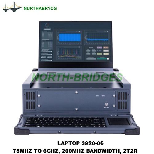
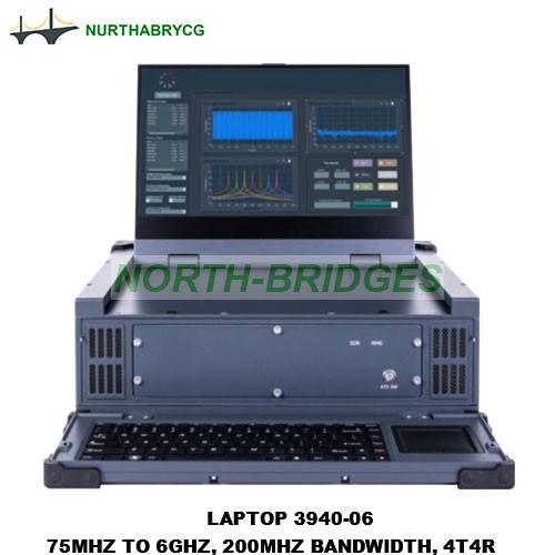
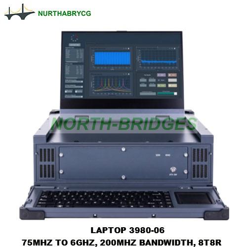
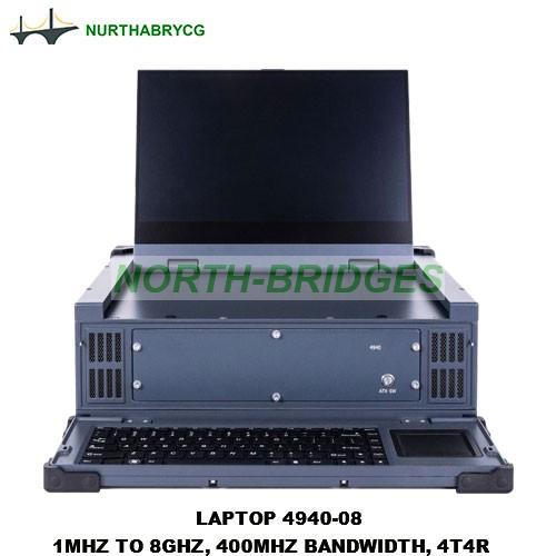
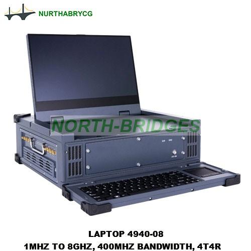
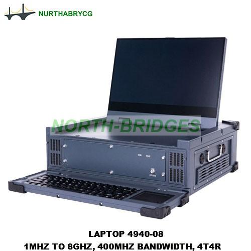
2974note / 3920note / 3940note / 3980note / 4940note
Pinout
Use the pinout to connect to terminals on the SDR Stand-Alone 2974 note.
Front Panel
| Table 1. Connector Descriptions | |||||||||
| Connector | Use | ||||||||
| RF 0 | TX1 RX1 | Input and output terminal for the RF signal. TX1 RX1 is an SMA (f) connector with an impedance of 50 Ω and is a single-ended input or output channel. | |||||||
| RX2 | Input terminal for the RF signal. RX2 is an SMA (f) connector with an impedance of 50 Ω and is a single-ended input channel. | ||||||||
| AUX I/O | General-purpose I/O (GPIO) port. AUX I/O is controlled by the FPGA. | ||||||||
| RF 1 | TX1 RX1 | Input and output terminal for the RF signal. TX1 RX1 is an SMA (f) connector with an impedance of 50 Ω and is a single-ended input or output channel. | |||||||
| RX2 | Input terminal for the RF signal. RX2 is an SMA (f) connector with an impedance of 50 Ω and is a single-ended input channel. | ||||||||
| DP | DisplayPort connector to connect one monitor for your controller. | ||||||||
| USB2.0 | USB ports that support common USB peripheral devices such as flash drives, hard drives, keyboards, and mice. | ||||||||
| USB3.0 | USB ports that support common USB peripheral devices such as flash drives, hard drives, keyboards, and mice. | ||||||||
| 1G ETH | RJ45 port used for 1G ETH connectivity to other ethernet devices. | ||||||||
| μUSB | USB port used for UART connectivity to the controller. | ||||||||
| 1G/10G ETH0 | SFP+ port used for 10G ETH connectivity to other ethernet devices. Connects to the embedded Linux computer for communication with LabVIEW RT. | ||||||||
| 1G/10G ETH1 | SFP+ port used for 1G/10G ETH connectivity to other ethernet devices. Connects to the FPGA. Not currently supported in LabVIEW Communications System Design Suite. | ||||||||
| Table 2. LEDs | |||||||||
| LED | Description | Color | State | Indication | |||||
| REF | Indicates the status of the reference signal. | OFF | - | There is no reference signal, or the device is not locked to the reference signal. | |||||
| Green | Blinking | The device is not locked to the reference signal. | |||||||
| Solid | The device is locked to the reference signal. | ||||||||
| PPS | Indicates the pulse per second (PPS). | OFF | - | There is no PPS timing reference signal, or the device is not locked to the reference signal. | |||||
| Green | Blinking | The device is locked to the PPS timing reference signal. | |||||||
| GPS | Indicates whether the GPSDO is locked. | OFF | - | There is no GPSDO or the GPSDO is not locked. | |||||
| Green | Solid | The GPSDO is locked. | |||||||
| STATUS | Indicates the status of the device. | OFF | - | The device initialized successfully and is ready for use. | |||||
| Red | Blinking | Hardware error. An internal power supply has failed. Check front-panel I/O connections for shorts. Remove any shorts and cycle power to the SDR Stand-Alone 2974. Contact NORTHBRIDGES if the problem persists. | |||||||
| PWR | Indicates the power status of the device. | OFF | - | The device is powered off. | |||||
| Green | Solid | The device is powered on. | |||||||
| 10/100/1000 | Indicates the speed of the Gigabit Ethernet link. | OFF | - | No link, or 10 Mbps link. | |||||
| Green | Solid | 100 Mbps link. | |||||||
| Amber | Solid | 1,000 Mbps link. | |||||||
| ACT/LINK | Indicates the Gigabit Ethernet link activity or status. | OFF | - | No link has been established. | |||||
| Green | Solid | A link has been negotiated. | |||||||
| Blinking | Activity on the link. | ||||||||
| 1G/10G ETH0 | ACT/LINK | Indicates the status of the SFP+ port. | OFF | - | The link is down. | ||||
| Green | Solid | The link is up. | |||||||
| Blinking | The link is active (transmitting and receiving). | ||||||||
| 10GbE | Indicates the status of the 10G ETH link. | OFF | - | The 10G ETH link is down. | |||||
| Green | Solid | The 10G ETH link is up. | |||||||
1G/10G ETH1 10GbE | Indicates the status of the 10G ETH link. | OFF | - | The 10G ETH link is down. | |||||
| Green | Solid | The 10G ETH link is up. | |||||||
Back Panel
| Table 3. Connector Descriptions | |||||||||
| Connector | Use | ||||||||
| REF OUT | Output terminal for an external reference signal for the LO on the device. REF OUT is an SMA (f) connector with an impedance of 50 Ω, and it is a single-ended reference output. The output signal at this connector is 10 MHz at 3.3 V. | ||||||||
| REF IN | Input terminal for an external reference signal for the LO on the device. REF IN is an SMA (f) connector with an impedance of 50 Ω, and it is a single-ended reference input. REF IN accepts a 10 MHz signal with a minimum input power of 0 dBm (0.632 V pk-pk) and a maximum input power of 15 dBm (3.56 V pk-pk) for a square wave or sine wave. | ||||||||
| PPS TRIG OUT | Output terminal for the PPS timing reference. PPS TRIG OUT is an SMA (f) connector with an impedance of 50 Ω and is a single-ended input. The output signal is 0 V to 3.3 V TTL. You can also use this port as a triggered output (TRIG OUT) that you program with the PPS Trig Out I/O signal. | ||||||||
| PPS TRIG IN | Input terminal for PPS timing reference. PPS TRIG IN is an SMA (f) connector with an impedance of 50 Ω and is a single-ended input channel. PPS TRIG IN accepts 0 V to 3.3 V TTL and 0 V to 5 V TTL signals. You can also use this port as a triggered input (TRIG IN) that you control using NI-USRP software. | ||||||||
| GPS ANT | Input terminal for the GPS antenna signal. GPS ANT is an SMA (f) connector with a maximum input power of -15 dBm and an output of 5 V DC to power an active antenna. | ||||||||
| Notice Do not terminate the GPS ANT port if you do not use it. | |||||||||
| PCIe x4 | Port for a PCI Express Generation 2, x4 bus connection through an MXI Express four-lane cable. Can be used to connect an external USRP device or external chassis. | ||||||||
| SYSTEM POWER IN | Input that accepts a 15 V ± 5%, 10 A external DC power connector. | ||||||||
Controller
| Note 2974-06 | Note 3920-06 | Note 3940-06 | Note 3980-06 | Note 4940-08 | |
| OS | Linux | Ubuntu | Ubuntu | Ubuntu | Ubuntu |
| CPU | I7 9700 | I9 12900 | I9 12900 | I9 12900 | I9 12900 |
| Memory | 16G | 64G | 64G | 64G | 64G |
| NVMe SSD | 500GB | 2TB | 2TB | 2TB | 2TB |
| RJ45 | 1Gbps | - | - | - | - |
| SFP | 4Gbps | 4Gbps | 4Gbps | ||
| SFP+ | 10Gbps | ||||
| QSFP28 | 100Gbps | ||||
| Cabled PCIe | PCIe Gen2 x4 | PCIe Gen3 x8 | PCIe Gen3 x8 | PCIe Gen3 x8 | PCIe Gen3 x8 |
| MicroUSB | USB3.0 x 4 | USB3.0 x 4 | USB3.0 x 4 | USB3.0 x 4 | USB3.0 x 4 |
FPGA and Baseband
| Note 2974-06 | Note 3920-06 | Note 3940-06 | Note 3980-06 | Note 4940-08 | |
| FPGA | Kintex-7XC7K410T | MPSoC ZU11EG | MPSoC ZU11EG | MPSoC ZU11EG | RFSoCXCZU28DR |
| DRAM | 1G | PS: 4GB DDR4 PL: 2GB DDR4 | PS: 4GB DDR4, PL: 2GB DDR4 | PS: 4GB DDR4, PL: 2GB DDR4 | PS: 4GB DDR4, PL: 8GB DDR4 |
| ADC resolution | 14 bits | 16 bits | 16 bits | 16 bits | 12 bits |
| DAC resolution | 16 bits | 14 bits | 14 bits | 14 bits | 14 bits |
| Maximum I/Q sample rate | 200 MSps | 400 MSps | 400 MSps | 400 MSps | 800 MSps |
RF
Transmitter
| Note 2974-06 | Note 3920-06 | Note 3940-06 | Note 3980-06 | Note 4940-08 | |
| Number of channels | 2 | 2 | 4 | 8 | 4 |
| Frequency range | 10MHz~6GHz | 75MHz~6GHz | 75MHz~6GHz | 75MHz~6GHz | 1MHz~7.2GHz (overclocking up to 8GHz) |
| Frequency step | <1kHz | <1kHz | <1kHz | <1kHz | <1kHz |
| Maximum output power (Pout) | 19.5dBm | 20dBm | 20dBm | 20dBm | 21dBm |
| Gain range | 0~31.5dB | 0~30dB | 0~30dB | 0~30dB | 0~60dB |
| Gain step | 0.5dB | 1dB | 1dB | 1dB | 1dB |
| Maximum instantaneous real-time bandwidth | 160 MSps | 450 MSps | 450 MSps | 450 MSps | 400 MSps |
Receiver
| Note 2974-06 | Note 3920-06 | Note 3940-06 | Note 3980-06 | Note 4940-08 | |
| Number of channels | 2 | 2 | 4 | 8 | 4 |
| Frequency range | 10MHz~6GHz | 75MHz~6GHz | 75MHz~6GHz | 75MHz~6GHz | 1MHz~7.2GHz (overclocking up to 8GHz) |
| Frequency step | <1kHz | <1kHz | <1kHz | <1kHz | <1kHz |
| Maximum input power (Pin) | -15dBm | -15dBm | -15dBm | -15dBm | <0dBm |
| Gain range | 0~31.5dB | 0~31.5dB | 0~31.5dB | 0~31.5dB | 38dB (<500GHz), 60dB (>500GHz) |
| Gain step | 0.5dB | 0.5dB | 0.5dB | 0.5dB | 1dB |
| Maximum instantaneous real-time bandwidth | 160 MSps | 200 MSps | 200 MSps | 200 MSps | 400 MSps |
| Noise figure | 5dB to 7dB | 6.5dB to 9dB | |||
GPS Disciplined Oscillator (GPSDO)
| Note 2974-06 | Note 3920-06 | Note 3940-06 | Note 3980-06 | Note 4940-08 | |
Local Oscillator Accuracy | |||||
Peripheral Oscillator | Support | Support | Support | Support | Support |
Peripheral PPS | Support | Support | Support | Support | Support |
Note: Frequency accuracy is based on temperature compensated crystal oscillator (TCXO) vendor specifications and is not measured. Alternatively, you can incorporate an external reference source to provide a more precise frequency Reference Clock and to achieve better frequency accuracy.
| Active Antenna | |||||
| Note 2974-06 | Note 3920-06 | Note 3940-06 | Note 3980-06 | Note 4940-08 | |
| Embedded | None | None | None | None | None |
| Peripheral | Support | Support | Support | Support | Support |
Note: NORTHBRIDGES recommends periodically locking the GPS for at least 1 hour to recalibrate the GPSDO module accuracy.
Power Requirements
Notice: The protection provided by this product may be impaired if it is used in a manner not described in this document.
| Note 2974-06 | Note 3920-06 | Note 3940-06 | Note 3980-06 | Note 4940-08 | |
| Input voltage | 220V | 220V | 220V | 220V | 220V |
| Input current | Maximum 16A | Maximum 16A | Maximum 16A | Maximum 16A | Maximum 16A |
Notice: The power supply must also meet any safety and compliance requirements for the country of use.
Physical Characteristics
If you need to clean the module, wipe it with a dry towel.
| Note 2974-06 | Note 3920-06 | Note 3940-06 | Note 3980-06 | Note 4940-08 | |
Dimensions, enclosure | 43×30×13.5 cm | 72.8×48.2×17.7 cm | 72.8×48.2×17.7 cm | 72.8×48.2×17.7 cm | 43×37.8×14.5 cm |
| Weight | 9.5Kg | 11.5Kg | 11.5Kg | 11.5Kg | 13.6Kg |
Environmental Characteristics
| Note 2974-06 | Note 3920-06 | Note 3940-06 | Note 3980-06 | Note 4940-08 | |
Operating temperature | 0 °C to 50 °C | ||||
| Operating humidity | 10% to 90% relative humidity, noncondensing | ||||
| Pollution Degree | 2 | ||||
| Maximum altitude | 2,000 m | ||||
Contact: Windy Lian
Phone: 13862120662
E-mail: sales@north-bridges.com
Whatsapp:
Add: Suzhou City, China
We chat