sales@north-bridges.com
86-13862120662
Disclaimer:
Product specifications on the website are for reference only, subject to the latest manufacturer-confirmed datasheet. Please contact us for official technical documents before project evaluation and quotation.
Operating system, BSP, drivers and SDK vary by hardware batch. Please contact us for official software compatibility documents before project development.
6U VPX High-Performance FPGA Boards
Covering UltraScale+ & legacy mainstream FPGAs, this lineup includes standalone FPGA, FPGA+DSP heterogeneous and MPSoC integrated platforms.
Capable of high-speed AD/DA, real-time RF processing, spectrum monitoring, multi-beam and parallel embedded computing.
Rugged wide-temperature compliant for industrial test, wireless communication, radar baseband and high-reliability embedded systems.
Product Selection Table
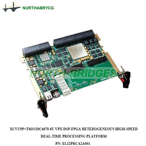
| Part Number | Main FPGA Chip | Auxiliary Processor | RF/Analog Interface | Max Transmission Bandwidth | Onboard Memory | High-speed Interface | Power Consumption | Operating Temperature | Application Scenario |
| EL12PRCA2A001 | XCVU9P | TMS320C6678 | 2 × FMC HPC for ADC/DAC/RF | QSFP+ (25G×4), SRIO ×4, 52 GTY | DSP: 2GB DDR3; FPGA: 2×2GB DDR4 | 40G QSFP+, SRIO, GTY | 50W @12V DC | -40℃ ~ +85℃ | High-speed acquisition, Real-time signal processing, SDR |
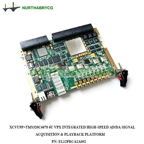
| EL12PRCA2A002 | XCVU9P | TMS320C6678 AD9689(ADC) AD9172(DAC) | 4CH ADC (3GSPS @14bit), 8CH DAC (3GSPS @16bit), Synchronous clock | QSFP28 40G, SRIO ×4, GTY | DSP: 2GB DDR3; FPGA: 2×2GB DDR4 | 40G QSFP28, SRIO, GTY, Gigabit Ethernet | 50W @12V DC | -40℃ ~ +85℃ | High-speed signal acquisition & playback, Wireless simulation, SDR |
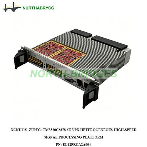
| EL12PRCA2A004 | XCKU115 | XCZU9EG TMS320C6678 | 2 × FMC+ (VITA57.4) for ADC/DAC/RF | SRIO 5Gbps/lane, PCIe Gen3 x4 | DSP: 4GB DDR3, + 4GB Nand Flash; FPGA/MPSoC: DDR4 /DDR3 | SRIO, PCIe Gen3, GTH | Max 5A @12V | -40℃ ~ +85℃ | Radar baseband processing, SDR |
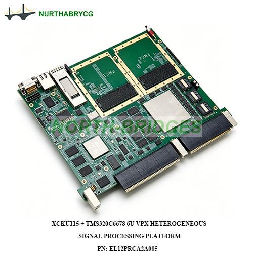
| EL12PRCA2A005 | XCKU115 | TMS320C6678 STM32 | 2 × FMC+ (VITA57.4) for ADC/DAC/RF | SRIO, EMIF, QSFP+ 40Gbps | FPGA: 2×4GB DDR4; DSP: 4GB DDR3 | SRIO, 40G QSFP+, EMIF | Max 5A @12V | -40℃ ~ +85℃ | Radar, SDR, Dedicated floating-point signal processing |
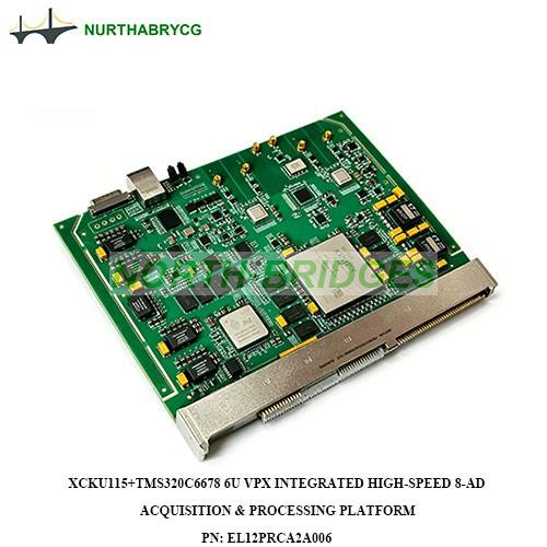
| EL12PRCA2A006 | XCKU115 (Optional XCKU085) | TMS320C6678 AD9689(ADC) | 8CH ADC, 14bit, 2.6GSPS max sampling rate | SRIO ×4, PCIe ×4, LVDS | FPGA: 4GB DDR4; DSP: 2GB DDR3 | SRIO, PCIe, LVDS, Gigabit Ethernet | <60W @12V DC | -20℃ ~+65℃ | High-speed acquisition, Real-time processing, Test & measurement, Radio frequency signal processing |
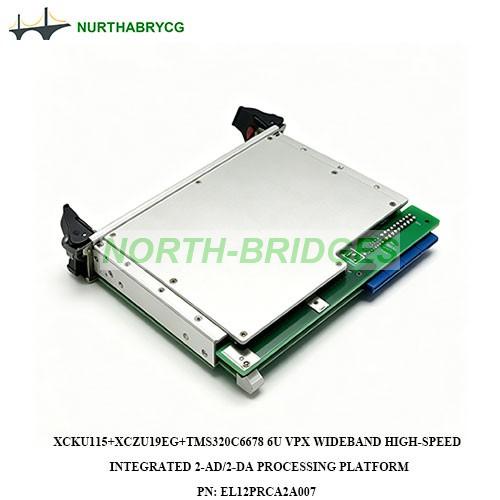
| EL12PRCA2A007 | XCKU115 | XCZU19EG TMS320C6678 | 2CH ADC (3.0GSPS @14bit), 2CH DAC (3GS/s @16bit) | PCIe 3.0 ×8 / ×4 | 2GB DDR4, 6GB DDR4, 2GB DDR3; 1Gb Boot Flash | PCIe 3.0 | 12V DC | -20℃ ~+65℃ | Integrated acquisition & generation, SDR, Physical experiment, Radio frequency signal processing |
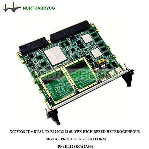
| EL12PRCA2A008 | XC7VX690T | Dual TMS320C6678 | 2 × FMC HPC for ADC/DAC/RF | HyperLink 5Gbps/lane, SRIO 5Gbps/lane, PCIe Gen2 x4 8Gbps | DSP: 4GB DDR3 + 4GB Nand Flash; FPGA: 2×2GB DDR3 | SRIO, HyperLink, PCIe Gen2, GTH | Max 5A @12V | -40℃ ~ +85℃ | Radar baseband processing, SDR |
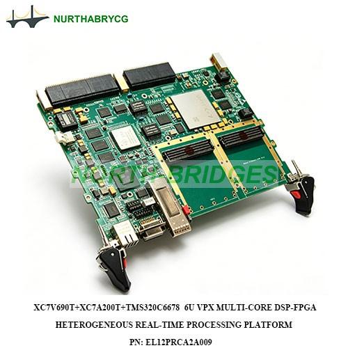
| EL12PRCA2A009 | XC7V690T | TMS320C6678 XC7A200T | 2 × FMC HPC for ADC/DAC/RF | 40G QSFP+, SRIO x4, PCIe x2 | DSP 2GB DDR3; FPGA 8GB DDR3 | 40G QSFP+, SRIO, PCIe, Gigabit Ethernet | 40W @12V | -40℃ ~ +85℃ | Real-time signal computing, Wireless communication |
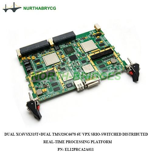
| EL12PRCA2A011 | Dual XC6VSX315T | Dual TMS320C6678 | 2×FMC HPC for AD/DA & image acquisition | SRIO switching network, HyperLink, GTX, LVDS | Each DSP: 2GB DDR3; Each FPGA: 2GB DDR3 + Flash | SRIO, HyperLink, GTX, LVDS, Gigabit Ethernet | 50W | -40℃ ~ +85℃, Hot-swap supported | Distributed parallel computing, SDR, Image processing |
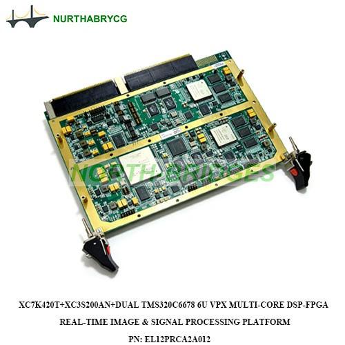
| EL12PRCA2A012 | XC7K420T | Dual TMS320C6678, XC3S200AN | No onboard RF, expandable via VPX backplane | HyperLink ×4, SRIO ×4, GTX, LVDS | Each DSP: 2GB DDR3; FPGA: DDR3 | HyperLink, SRIO, GTX, LVDS, 4×Gigabit Ethernet | 12V@6A + 5V@1A | -40℃ ~ +85℃ | Image processing, Real-time signal computing, Embedded wireless system |
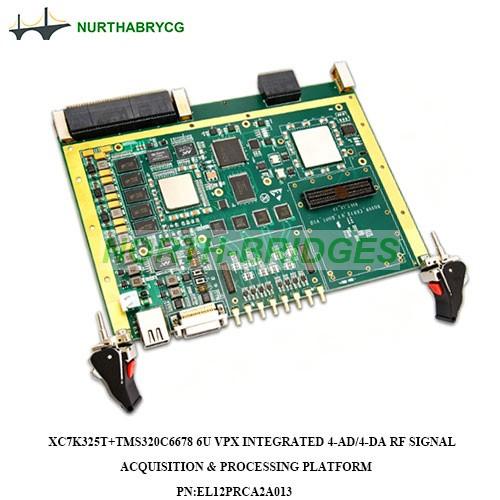
| EL12PRCA2A013 | XC7K325T | TMS320C6678 AD9652(ADC) AD9122(DAC) | 4CH ADC, 4CH DAC, Intermediate frequency RF channel | SRIO ×4, GTX ×8, LVDS, PCIe | DSP: DDR3 + Nor Flash; FPGA: BPI Flash | SRIO, GTX, LVDS, PCIe, 2×Gigabit Ethernet | 12V DC | -40℃ ~ +85℃ | RF signal acquisition & processing, Radio communication |
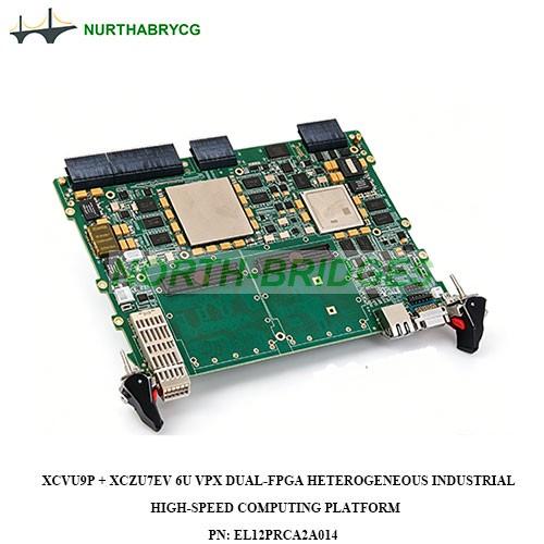
| EL12PRCA2A014 | XCVU9P | XCZU7EV | 2 × FMC HPC for AD/DA/RF | QSFP28 (25G×4), SRIO x4, 52 GTY | Main: 2×8GB DDR4; Aux: PS 2GB + PL 2GB DDR4 | QSFP28, SRIO, GTY, L VDS, CAN, USB3.0 | 120W @12V | -40℃ ~ +85℃ | High-speed computing, Fiber acceleration, SDR, Image processing |
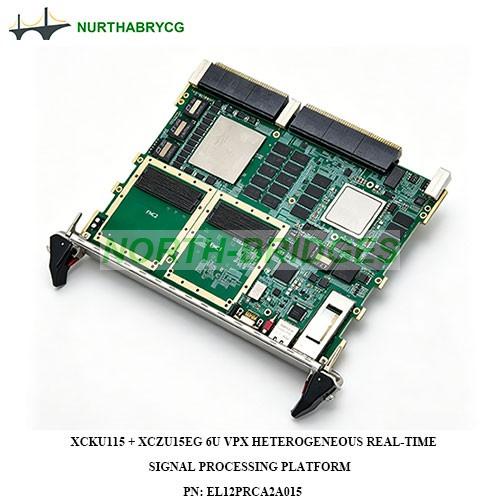
| EL12PRCA2A015 | XCKU115 | XCZU15EG | 2 × FMC+ (VITA57.4) for ADC/DAC/RF | 4 × SRIO x4, QSFP+ 40Gbps, 8 GTH @16Gbps | FPGA/MPSoC: DDR4-2400 | SRIO, 40G QSFP+, GTH, LVDS | Max 5A @12V | -40℃ ~ +85℃ | High-throughput signal processing, SDR, Radar |
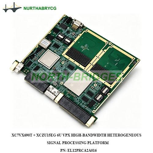
| EL12PRCA2A016 | XC7VX690T | XCZU15EG | 2 × FMC + (VITA57.4) for ADC/DAC/RF | 4 × SRIO x4, Quad optical ports, 16 GTH transceivers | FPGA: 2×4GB DDR3 + 128MB BPI Flash; MPSoC: DDR4 | SRIO, Optical, GTH, LVDS, Gigabit Ethernet | Max 5A @12V | -40℃ ~ +85℃ | High-bandwidth radar, SDR |
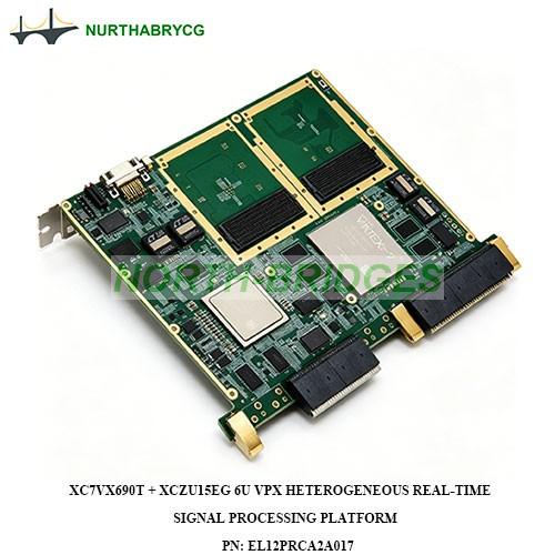
| EL12PRCA2A017 | XC7VX690T | XCZU15EG | 2 × FMC+ (VITA57.4) for ADC/DAC/RF | 3 × SRIO x4, 16 GTH transceivers | FPGA: 2×4GB DDR3 + 128MB BPI Flash; MPSoC: DDR4 | SRIO, GTH, LVDS, Gigabit Ethernet | Max 5A @12V | -40℃ ~ +85℃ | Radar baseband processing, SDR |
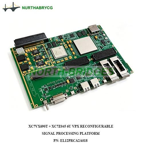
| EL12PRCA2A018 | XC7VX690T | XC7Z045 | 1 × FMC HPC, 2 × FMC+ HPC for AD/DA/RF | 2 × QSFP+, OCXO multi-clock synchronization | ≥16GB QRAM, ≥32MB Flash | QSFP+, Gigabit Ethernet, UART, GPIO | Typical 140W | -40℃ ~ +55℃ | Massive MIMO, BBU, Channel simulator, Telecom & Defense |
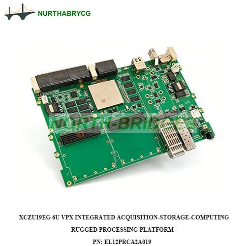
| EL12PRCA2A019 | XCZU19EG | N/A | 2 × FMC HPC for AD/DA/RF | 2 × 100G QSFP28, PCIe Gen3 x8 | PS 4GB DDR4; PL 4GB DDR4 | 100G QSFP28, PCIe Gen3, GTH, LVDS | 60W @12V | -40℃ ~ +85℃ | All-in-one acquisition, storage & real-time computing |
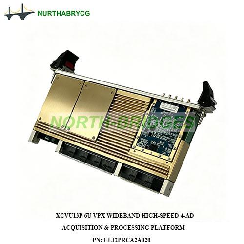
| EL12PRCA2A020 | XCVU13P | N/A | 4CH ADC, 14bit, 3.0GSPS, 9GHz analog bandwidth | High-speed transceiver, Backplane links | 8GB DDR4; 2×1Gb QSPI Flash | High-speed GT transceivers | 12V DC | -20℃ ~+65℃ | Wideband signal acquisition, SDR, Test & measurement, Radio frequency signal processing |
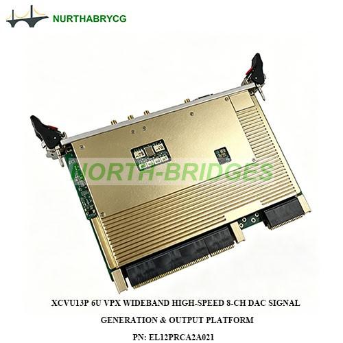
| EL12PRCA2A021 | XCVU13P | N/A | 8CH DAC, 16bit, 3GS/s per channel | PCIe 3.0 ×16, SRIO ×2 | 8GB DDR4 | PCIe 3.0, SRIO | 12V DC | -20℃ ~+65℃ | Multi-channel signal generation, Digital beamforming, MIMO, Radio frequency signal processing |
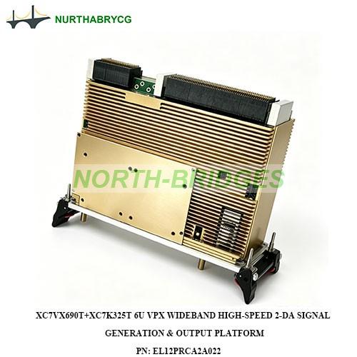
| EL12PRCA2A022 | XC7VX690T XC7K325T (Dual FPGA) | N/A | 2CH DAC, 16bit, 3GS/s~6GS/s output | PCIe 2.0 ×8 | 4GB DDR3; Dual 256Mb SPI Flash | PCIe 2.0 | 12V DC | -20℃ ~+65℃ | Wideband signal generation, Wireless communication, Test instrument, Radio frequency signal processing |
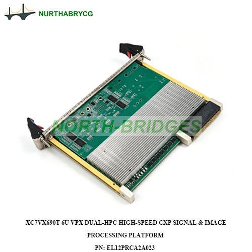
| EL12PRCA2A023 | XC7VX690T | N/A | 2×HPC FMC for ADC/DAC/RF /camera | CXP 3.125Gbps, PCIe, GTX | 8×DDR3; 1Gb Parameter Flash, 256Mb Program Flash | CXP, PCIe, GTX | ≤30W @12V DC | -10℃ ~ +60℃ | Radar signal preprocessing, High-speed image processing |
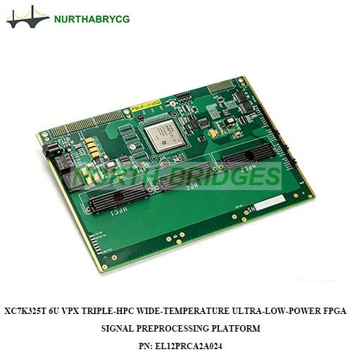
| EL12PRCA2A024 | XC7K325T | N/A | 3×HPC FMC for ADC/DAC/RF /sensor | LVDS, Backplane high-speed links | 4×DDR3; 1Gb Flash, 256Mb Flash, 2Mb EEPROM | LVDS, RS422 | ≤1W @12V DC | -40℃ ~ +60℃ | Ultra-low-power acquisition, Harsh environment embedded system |
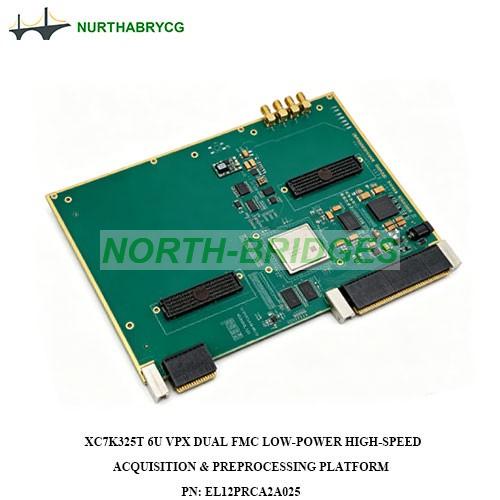
| EL12PRCA2A025 | XC7K325T | N/A | 1×Standard HPC, 1×Custom HPC for ADC/DAC/RF /sensor | GTX via BNC, LVDS | 4×DDR3; 1Gb Flash, 256Mb Flash, 2Mb EEPROM | GTX, LVDS, RS422 | ≤5W @12V DC | -10℃ ~ +60℃ | Low-power signal acquisition, Multi-sensor preprocessing |
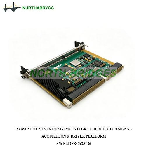
| EL12PRCA2A026 | XC6SLX100T | N/A | 2×FMC for high-speed ADC; 8CH analog acquisition | GTP, LVDS | 2×DDR3 | GTP, LVDS | ≤3W | -30℃ ~ +55℃ (Extend: -40℃ ~ +85℃) | Detector signal acquisition, Power driving, Aerospace & nuclear detection |
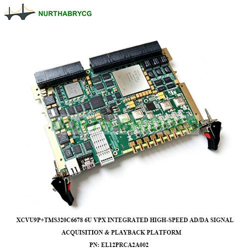
PN.: EL12PRCA2A002
XCVU9P+TMS320C6678 6U VPX Integrated High‑Speed AD/DA Signal Acquisition & Playback Platform
Specifications
| Form Factor | 6U VPX | ||||||||
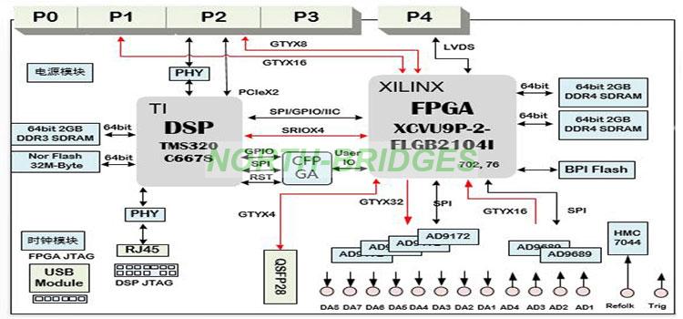
| Chip | TMS320C6678 + XCVU9P + AD9689 ADC + AD9172 DAC | ||||||||
| Memory | DSP: 2GB DDR3 | ||||||||
| FPGA: 2×2GB DDR4 | |||||||||
| RF Channel | ADC: 4CH, 3GSPS,14bit | ||||||||
| DAC: 8CH, 3GSPS,16bit | |||||||||
| I/O | 40G QSFP28, SRIO×4, GTY transceivers | ||||||||
| Peripherals | GbE, SPI, GPIO, IIC, JTAG, USB | ||||||||
| Power | 12V DC, 50W | ||||||||
| Operation Temp. | -40℃~+85℃ | ||||||||
Block Diagram
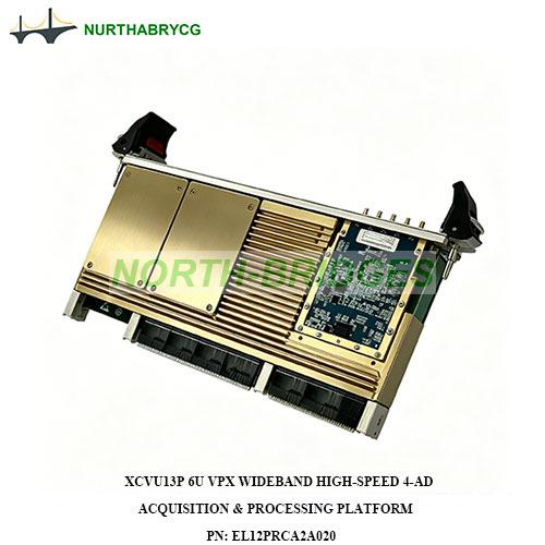
PN.: EL12PRCA2A020
XCVU13P 6U VPX Wideband High-Speed 4‑AD Acquisition & Processing Platform
Specifications
| Form Factor | 6U VPX | ||||||||
| Chip | XCVU13P, pin compatible with VU9P/VU11P | ||||||||
| ADC | 4CH,14bit, max3.0/2.6/2.0GSPS | ||||||||
| Analog Bandwidth | -3dB full-power up to 9GHz | ||||||||
| Input Mode | Default AC-coupled, DC-coupling hardware ready | ||||||||
| Memory | 8GB total DDR4 | ||||||||
| 2×1Gb QSPI Flash | |||||||||
| Operation Temp. | -20℃~+65℃ | ||||||||
Block Diagram

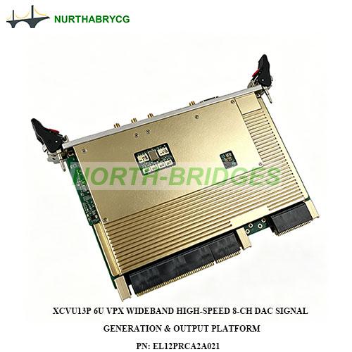
PN.: EL12PRCA2A021
XCVU13P 6U VPX Wideband High-Speed 8‑CH DAC Signal Generation & Output Platform
Specifications
| Form Factor | 6U VPX | ||||||||
| Chip | XCVU13P, pin compatible with VU9P/VU11P | ||||||||
| DAC | 8CH,16bit, AC-coupled | ||||||||
| Update Rate | Real: 8×3GSPS (verified 8×1.2GSPS) | ||||||||
| Complex: max12.6GSPS | |||||||||
| Memory | 8GB DDR4 | ||||||||
| Backplane | 4×SRIO×2, PCIe3.0×16 | ||||||||
| Operation Temp. | -20℃~+65℃ | ||||||||
Block Diagram

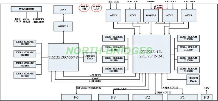
PN.: EL12PRCA2A006
XCKU115+TMS320C6678 6U VPX Integrated High-Speed 8‑AD Acquisition & Processing Platform

Specifications
| Form Factor | 6U VPX | ||||||||
| Chip | XCKU115 (optional XCKU085)+TMS320C6678+AD9689 ADC | ||||||||
| ADC | 8CH,14bit, max 2.6GSPS | ||||||||
| SMA/SMP interface | |||||||||
| Memory | FPGA: 4GB DDR4 | ||||||||
| DSP: 2GB DDR3 | |||||||||
| Front Panel | 1×GbE, 1×J30J(JTAG+4GPIO+4RS422), 1×SMA/SMP clock | ||||||||
| Backplane | P1: 4×SRIO×4@5Gbps | ||||||||
| P2: PCIe×4@5Gbps | |||||||||
| P3: 22×LVDS | |||||||||
| P6: 8GPIO+4RS422 | |||||||||
| Power | 12V VPX-P0 input, total<60W | ||||||||
Block Diagram
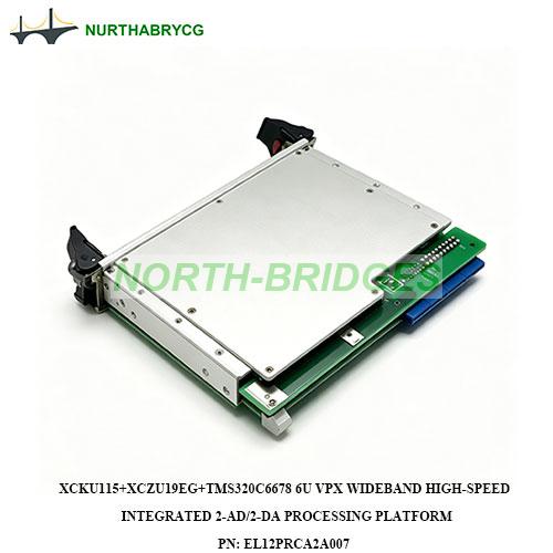
PN.: EL12PRCA2A007
XCKU115+XCZU19EG+TMS320C6678 6U VPX Wideband High-Speed Integrated 2‑AD/2‑DA Processing Platform
Specifications
| Form Factor | 6U VPX | ||||||||
| Chip | XCKU115+XCZU19EG+TMS320C6678 | ||||||||
| ADC | 2CH,14bit, AC-coupled, SSMC, 2.6/3.0GSPS | ||||||||
| DAC | Real: 2×3GSPS/1×6GSPS | ||||||||
| Complex: max12.6GSPS | |||||||||
| Memory | 2GB DDR4,4GB+2GB DDR4,2GB DDR3; | ||||||||
| Total 1Gbit Boot Flash | |||||||||
| Backplane | 2×PCIe3.0×8 | ||||||||
| 2×PCIe3.0×4 | |||||||||
Block Diagram

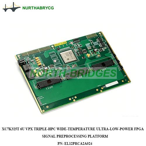
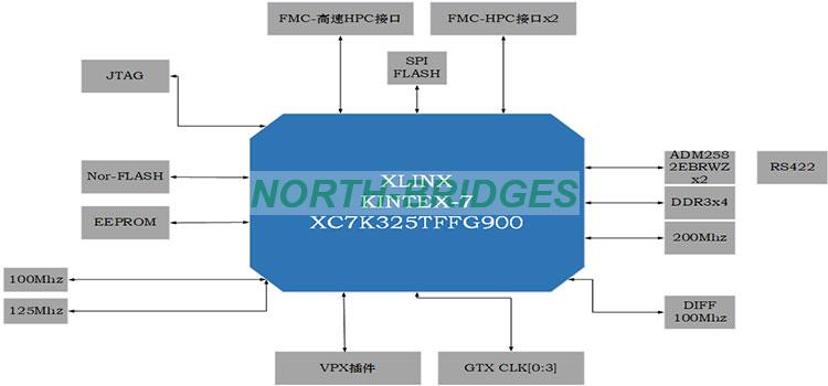
PN.: EL12PRCA2A024
XC7K325T 6U VPX Triple‑HPC Wide-Temperature Ultra-Low-Power FPGA Signal Preprocessing Platform
Specifications
| Form Factor | 6U VPX | ||||||||
| Chip | XC7K325T | ||||||||
| FMC | 2HPC, 1HSPC | ||||||||
| I/O: 1.2/1.5/1.8/2.5/3.3V adjustable | |||||||||
| Memory | 4×DDR3,1Gb Param Flash, 256Mb Prog Flash, 2Mbit EEPROM | ||||||||
| Clock | Single-ended 100MHz, Diff 100/200MHz | ||||||||
| Peripherals | 2×Isolated ESD RS422, protected JTAG | ||||||||
| Power | 12V DC with OVP, ≤1W | ||||||||
| Operation Temp. | -40℃~+60℃ | ||||||||
Block Diagram
PN.: EL12PRCA2A011
Dual XC6VSX315T+Dual TMS320C6678 6U VPX SRIO‑Switched Distributed Real‑Time Processing Platform
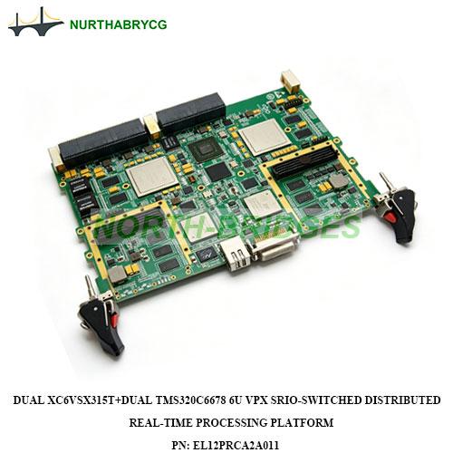
Specifications
| Form Factor | 6U VPX | ||||||||
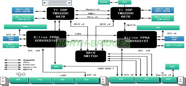
| Chip | 2×TMS320C6678 + 2×XC6VSX315T | ||||||||
| Memory | Each DSP: 2GB DDR3 | ||||||||
| Each FPGA: 2GB DDR3 | |||||||||
| Nor Flash, SPI FRAM | |||||||||
| I/O | SRIO×4 switching fabric, HyperLink, GTX, LVDS, PCIe, Gigabit Ethernet | ||||||||
| FMC | 2×HPC, VITA57.1 | ||||||||
| Power | +5V@5A & +3.3V@6A, 50W | ||||||||
| Operation Temp. | -40℃~+85℃ | ||||||||
Block Diagram
PN.: EL12PRCA2A026
XC6SLX100T 6U VPX Dual‑FMC Integrated Detector Signal Acquisition & Driver Platform
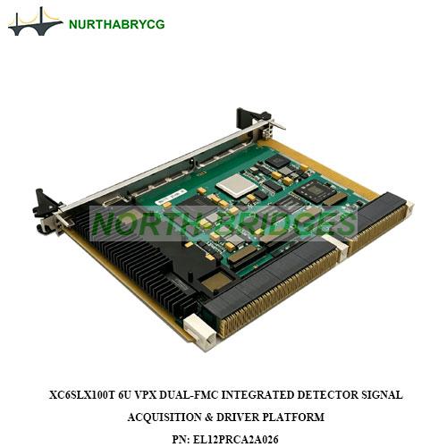
Specifications
| Form Factor | 6U VPX | ||||||||
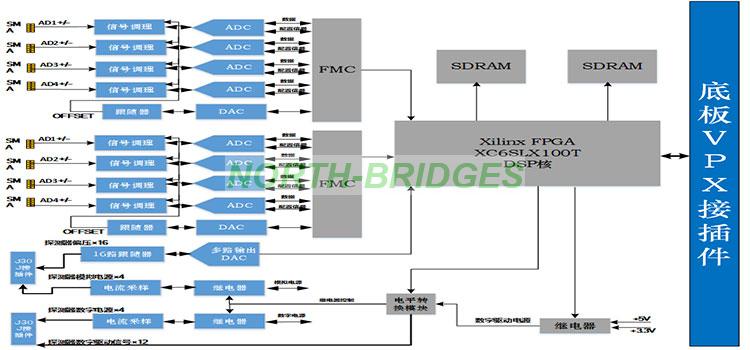
| Chip | XC6SLX100T | ||||||||
| FMC | VITA57.1, 2×HPC | ||||||||
| Each: 4ch-ADC or 32-Lanes LVDS | |||||||||
| Analog Input | 8ch, 0~5V, 18/24bit, max 10MHz sampling | ||||||||
| Power Output | 4ch Analog power | ||||||||
| 2ch Digital power | |||||||||
| 16ch Bias | |||||||||
| 12ch Digital drive | |||||||||
| Memory | DDR3, 2×2GB | ||||||||
| I/O | 6×LVDS or 8×GTP | ||||||||
| Power | +12V2A/, -5V1A, ≤3W | ||||||||
| Operation Temp. | -40℃~+85℃ | ||||||||
Block Diagram
Ordering
| PN: | All above | ||||||||
| Lead time: | Inquire for official quotation | ||||||||
| Custom designs: | Available upon request | ||||||||
| Support: | FPGA reference design, schematic review, driver development (quoted separately) | ||||||||
Contact: Windy Lian
Phone: 13862120662
E-mail: sales@north-bridges.com
Whatsapp:
Add: Suzhou City, China
We chat